
Expect to see China continue its strategy of incremental, targeted advancements across various segments of the chip supply chain, focusing on building out domestic capabilities in areas previously dominated by foreign suppliers. This Hwatsing development suggests a sustained effort to master foundational manufacturing processes, even if the immediate application is for less advanced chips. The broader industry will be watching to see how quickly these domestic technologies can scale up to larger wafer sizes and more complex manufacturing nodes, which remains a formidable technical and financial challenge. We can anticipate further announcements of specific equipment breakthroughs, alongside continued rapid expansion of existing fabrication capacity for mature and near-advanced chips.
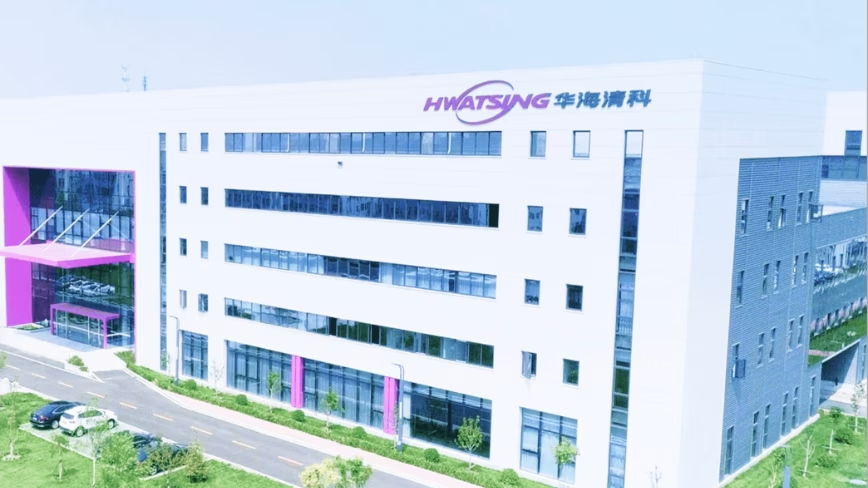
Image: courtesy of Thenextweb
China's Quiet Chip Breakthrough: The 6-Inch Wafer That Reveals Its Deeper Challenge
China's domestic semiconductor industry recently marked a significant, if understated, technical achievement: Hwatsing, a Chinese equipment maker, has developed the country's first integrated metrology system designed for wafer polishing equipment. This system is crucial for ensuring the ultra-flat surfaces needed in chip manufacturing. However, the system currently operates on six-inch wafers, a size largely used for mature chip technologies, rather than the twelve-inch wafers necessary for advanced logic chips. While this represents a concrete step towards domestic self-sufficiency in a critical fabrication step, it also highlights the persistent, complex hurdles China faces in fully closing the technology gap with leading global manufacturers, particularly in scaling to the cutting edge of semiconductor production.
Outlook
Background
The production of semiconductor chips is a multi-stage, highly precise process, and one of the most critical steps involves preparing the silicon wafer itself. Wafers must be polished to an atomic-level flatness to allow for the intricate layering of circuits. Metrology systems are the sophisticated measurement tools that inspect these wafers at every stage, ensuring they meet the impossibly tight specifications required. Without precise metrology, the entire manufacturing line grinds to a halt.
Hwatsing's breakthrough is in integrating this metrology directly with polishing equipment. This is important because it allows for real-time feedback and adjustment, improving efficiency and yield. Historically, such integrated systems have been dominated by non-Chinese firms, making this a notable step towards China's goal of domestic self-sufficiency in semiconductor equipment, which currently stands at around 35%.
However, the detail that often goes unmentioned is the wafer size. The system works on six-inch wafers. Modern, advanced logic chips – the kind found in smartphones, AI accelerators, and high-performance computing – are almost exclusively manufactured on twelve-inch wafers. These larger wafers allow for far more individual chips to be produced simultaneously, drastically reducing the per-chip cost and making advanced manufacturing economically viable. Six-inch wafers are typically used for older, less complex chips, such as those found in power management, automotive components, or certain sensors. While these 'legacy' chips are still vital, mastering their production does not equate to parity in cutting-edge logic.
China's broader push for self-reliance in semiconductors is aggressive. The country aims to achieve 70% domestic wafer supply by the end of this year, 2026. This ambition is supported by significant investment in domestic foundries like Semiconductor Manufacturing International Corp. (SMIC) and Hua Hong Semiconductor. SMIC, for instance, saw its output at seven nanometers (nm) and below reach an estimated 45,000 wafer starts per month in late 2025. Projections indicate this figure could hit 60,000 this year and 80,000 in 2027. Beijing has set an even more ambitious target for combined seven nm and five nm output to grow fivefold within two years, with Hua Hong expected to join SMIC in advanced production. These targets illustrate the sheer scale of the output China is trying to achieve, even as it grapples with the underlying equipment challenges.
Beyond polishing and metrology, China has also made strides in lithography, another bottleneck. On September 15, 2024, China announced advancements in domestic deep ultraviolet (DUV) lithography machines. One machine reportedly operates at a wavelength of 193 nm, achieving a resolution below 65 nm, while another has a 248 nm wavelength with 110 nm resolution. While DUV technology is foundational, it still trails the extreme ultraviolet (EUV) lithography used for the most advanced nodes by industry leaders like Taiwan Semiconductor Manufacturing Company (TSMC) and Samsung. This layered context of progress in some areas, alongside persistent gaps in others, defines the current state of China's chipmaking ambitions.
See also
Precedents
China's approach to closing technological gaps in critical industries has historically been characterized by sustained, state-backed investment and a focus on incremental, foundational progress. This is not a new playbook; it has been applied across various sectors, from high-speed rail to aerospace. The pattern often involves first mastering less complex components or processes, then systematically working up the value chain.
In semiconductors, this strategy has been evident for decades. Early efforts focused on assembly and packaging, then moved to design, and more recently, to fabrication and equipment. The current drive is a more intense, concentrated version of this long-standing policy, fueled by national security concerns and export controls from the U.S. and its allies. China's 'Deep Seek' initiative, mentioned in industry discussions, is another example of how domestic capabilities are cultivated over time, often out of public view, before emerging as significant achievements.
The challenge for China has always been less about individual breakthroughs and more about integrating a vast, complex ecosystem. Chipmaking requires thousands of highly specialized tools, materials, and processes, each with its own set of technical hurdles. Historically, no single nation has achieved complete self-sufficiency in this industry. China's current trajectory suggests a determination to build as much of this ecosystem domestically as possible, even if it means initially targeting mature technologies that are less reliant on foreign cutting-edge equipment.
The Hwatsing development, despite its focus on six-inch wafers, carries significant weight for several reasons.
First, it addresses a critical bottleneck in the chip manufacturing process. Wafer polishing metrology is a precision-intensive step, and developing a domestic solution reduces reliance on foreign suppliers for a fundamental piece of the fabrication puzzle. This enhances China's overall resilience against potential supply chain disruptions or further export controls.
Second, it signals a deeper institutional capability. Building complex, integrated systems, even for older technologies, demonstrates a growing pool of engineering talent and a maturing research and development infrastructure within China's semiconductor sector. This foundational knowledge can, in theory, be applied and scaled to more advanced systems over time. It suggests that China is not just trying to buy or reverse-engineer technology, but to innovate from the ground up in specific areas.
Third, for the global industry, China's progress, however incremental, means increasing competition and potential shifts in the supply chain. If China can reliably produce essential equipment for mature nodes, it could create a more fragmented market, potentially lowering costs for certain types of chips but also introducing new geopolitical complexities. Companies outside China may face pressure to diversify their own supply chains or confront a new domestic competitor.
Finally, for consumers and industries reliant on chips – which is almost every industry today – the implications are mixed. Greater self-sufficiency in China could stabilize the supply of 'legacy' chips, which are crucial for everything from automobiles to washing machines. However, if this comes at the cost of global collaboration and efficiency, it could also lead to higher costs or slower innovation for the most advanced computing technologies in the long run. The real stakes here are not just about who makes the fastest chip, but about the fundamental structure of the global technology supply chain and the geopolitical power balances it underpins.
Scenarios
AnalysisThe Hwatsing breakthrough, coupled with China's broader semiconductor strategy, suggests several potential outcomes for the industry:
* Accelerated Domestic Supply for Mature Nodes: China is likely to continue consolidating and expanding its domestic supply chain for mature chip technologies. The Hwatsing system, along with advancements in DUV lithography and increased capacity at SMIC for 7nm and above, indicates a deliberate strategy to achieve self-sufficiency in a wide array of chips that power everyday electronics and industrial applications. This could lead to China becoming a dominant force in the production of these 'legacy' chips, potentially creating a distinct, self-contained ecosystem less vulnerable to external pressures.
* Persistent Gap in Advanced Logic, But Narrowing in Specific Sub-Sectors: While Hwatsing's 6-inch wafer system does not immediately address the 12-inch advanced logic gap, the underlying metrology and polishing expertise is transferable. One possible outcome is that Chinese firms, with sustained state support, could leverage this foundational knowledge to develop 12-inch compatible integrated systems faster than anticipated. This would not necessarily mean parity with the most advanced foundries, but it would signify a significant narrowing of the gap in specific, highly technical equipment categories, reducing reliance on foreign giants like Applied Materials or Lam Research.
* Strategic Diversification of Global Supply Chains: The consistent pressure on China to develop domestic capabilities, and its measured successes, may prompt other nations and global chipmakers to further diversify their own supply chains. Rather than relying heavily on any single region for critical equipment or fabrication, companies could seek to establish production in multiple geographies. This could result in a more resilient, albeit potentially less efficient, global semiconductor industry, with regional hubs developing specialized expertise and capacity.
Timeline
Frequently Asked Questions
Discussion
Be the first to share your thoughts.